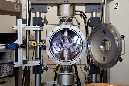
The Department of Materials Science disposes of a large and state-of-the-art technical infrastructure. The devices are used for research as well as for the students’ training.
General Materials Properties
- Heat treatments
- Metallography and sample preparation
- Microscopy and analysis
- Mechanical testing
- Tribological properties
- Generation of nanostructured materials
- Hydrogen analytics
- Simulation
- Other equipment
Materials Science and Engineering for Metals
- Primary shaping
- Additive Manufacturing
- Heat treatment
- Coating technology
- Mechanical Testing
- Physical, chemical and optical analysis
- Sample preparation
- Numerical simulation
Glass and Ceramics
(selection)
- Dilatometers (up to 1800 °C)
- Thermal analysis (DTA/TGA/DSC)
- Thermal conductivity device
- Powder X-ray diffractometer Bruker D8 Advanced Eco and Pro
- Gas absorption analyser (BET)
- ICP-OES (Spectro Analytical Instruments)
- Ball, vibration and attrition mills
- Kilns and Dryers (glass melting, high-temperature up to 2500 °C, vacuum)
- Tape caster and Fibre winding facilities
- Low-pressure injection moulding device
- High precision diamond wire saw
Polymers
- Rotation rheometer ARES
- Molecular Analyses: GPC1
- Karl-Fischer-Titration
- Differential scanning calorimetry
- Mechanical measurements
- Spritzgussmaschine (Arburg)
- Singlescrewextruder
- Twinscrewextruder with a Chill-roll-equipment
- Blown film unit
- Pilot fiber spinning line (Spunbond)
Materials for Electronics and Energy Technology
(selection)
- Aerosol Jet Platform
- Glovebox systems MBraun / Jacomex (GS Glovebox Systems)
- Robotic setup for automatic synthesis and characterization of solvent-preocessed semiconductors
- Spraycoating Setup (Single Head)
- Slot-die-Coater (FMP) (EnCN)
- Scanning electron microscope with CL and EDX (JEOL, JSM7610F)
- X-ray diffractometer (Panalytical)
- Particle size analyzer (Coulter LS100)
- Dynamic Light Scattering System (Nanoflex, Microtrack)
- UV-Vis absorption spectrometer, 190 – 3000 nm (Perkin Elmer Lambda 950)
- Photoluminescence setup, detection 300 – 1600 nm, excitation wavelengths 325, 375, 488, 514, 632, and 975 nm
- Photoinduced Absorption Setup (pump 532 and 785 nm, Probe 500 – 1700 nm)
- Flourometer FP-8500 (Jasco, excitation 200 – 600 nm, detection 300 – 850 nm)
- Timeresolved fluorometer (PicoQuant FL300)
- Kelvin-Probe with surface Photovoltage Spectroscopy option
- Contact angle measurement OCA 20
- AFM Mikcroscope ( NT-MDT )
Micro- and Nanostructure-Research